- 您现在的位置:买卖IC网 > Sheet目录508 > SI1469DH-T1-GE3 (Vishay Siliconix)MOSFET P-CH 20V SC-70-6
�� �
�
�AN815�
�Vishay� Siliconix�
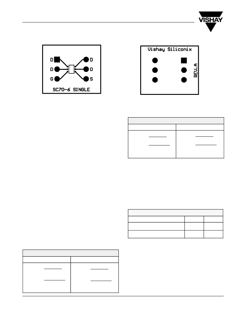
�Front� of� Board� SC70-6�
�Back� of� Board� SC70-6�
�vishay.com�
�FIGURE� 3.�
�THERMAL� PERFORMANCE�
�R� q� JA�
�P� D� +� 150� C� o� *� 25� C�
�R� q� JA�
�P� D� +� 150� C� o� *� 60� C�
�Junction-to-Foot� Thermal� Resistance�
�(Package� Performance)�
�The� junction� to� foot� thermal� resistance� is� a� useful� method� of�
�comparing� different� packages� thermal� performance.�
�A� helpful� way� of� presenting� the� thermal� performance� of� the�
�6-Pin� SC-70� copper� leadframe� device� is� to� compare� it� to� the�
�traditional� Alloy� 42� version.�
�COOPER LEADFRAM� E�
�Room� Ambient� 25� _� C�
�T� J(max)� *� T� A�
�P� D� +�
�o� o�
�124� C� W�
�P� D� +� 1.01� W�
�Elevated� Ambient� 60� _� C�
�T� J(max)� *� T� A�
�P� D� +�
�o� o�
�124� C� W�
�P� D� +� 726� mW�
�R� q� JA�
�R� q� JA�
�P� D� +� 150� C� o� *� 25� C�
�P� D� +� 150� C� o� *� 25� C�
�329.7� _� C/W�
�208.5� _� C/W�
�2)� Industry� standard� 1-inch� 2� PCB� with�
�211.8� _� C/W� 103.5� _� C/W�
�Thermal� performance� for� the� 6-pin� SC-70� measured� as�
�junction-to-foot� thermal� resistance,� where� the� “foot”� is� the�
�drain� lead� of� the� device� at� the� bottom� where� it� meets� the� PCB.�
�The� junction-to-foot� thermal� resistance� is� typically� 40� _� C/W� in�
�the� copper� leadframe� and� 163� _� C/W� in� the� Alloy� 42� leadframe�
�—� a� four-fold� improvement.� This� improved� performance� is�
�obtained� by� the� enhanced� thermal� conductivity� of� copper� over�
�Alloy� 42.�
�Power� Dissipation�
�The� typical� R� q� JA� for� the� single� 6-pin� SC-70� with� copper�
�leadframe� is� 103� _� C/W� steady-state,� compared� with� 212� _� C/W�
�for� the� Alloy� 42� version.� The� figures� are� based� on� the� 1-inch� 2�
�FR4� test� board.� The� following� example� shows� how� the� thermal�
�resistance� impacts� power� dissipation� for� the� two� different�
�leadframes� at� varying� ambient� temperatures.�
�ALLOY� 42� LEADFRAME�
�Room� Ambient� 25� _� C� Elevated� Ambient� 60� _� C�
�T� J(max)� *� T� A� T� J(max)� *� T� A�
�P� D� +� P� D� +�
�o� o� o� o�
�212� C� W� 212� C� W�
�P� D� +� 590� mW� P� D� +� 425� mW�
�www.vishay.com�
�2�
�As� can� be� seen� from� the� calculations� above,� the� compact� 6-pin�
�SC-70� copper� leadframe� LITTLE� FOOT� power� MOSFET� can�
�handle� up� to� 1� W� under� the� stated� conditions.�
�Testing�
�To� further� aid� comparison� of� copper� and� Alloy� 42� leadframes,�
�Figure� 5� illustrates� single-channel� 6-pin� SC-70� thermal�
�performance� on� two� different� board� sizes� and� two� different� pad�
�patterns.� The� measured� steady-state� values� of� R� q� JA� for� the�
�two� leadframes� are� as� follows:�
�LITTLE FOOT 6-PIN SC-7� 0�
�Alloy� 42� Copper�
�1)� Minimum� recommended� pad� pattern� on�
�the� EVB� board� V� (see� Figure� 3.�
�maximum� copper� both� sides.�
�The� results� indicate� that� designers� can� reduce� thermal�
�resistance� (R� q� JA� )� by� 36%� simply� by� using� the� copper�
�leadframe� device� rather� than� the� Alloy� 42� version.� In� this�
�example,� a� 121� _� C/W� reduction� was� achieved� without� an�
�increase� in� board� area.� If� increasing� in� board� size� is� feasible,�
�a� further� 105� _� C/W� reduction� could� be� obtained� by� utilizing� a�
�1-inch� 2� square� PCB� area.�
�The� copper� leadframe� versions� have� the� following� suffix:�
�Single:� Si14xxEDH�
�Dual:� Si19xxEDH�
�Complementary:� Si15xxEDH�
�Document� Number:� 71334�
�12-Dec-03�
�发布紧急采购,3分钟左右您将得到回复。
相关PDF资料
SI1470DH-T1-GE3
MOSFET N-CH 30V SC-70-6
SI1471DH-T1-GE3
MOSFET P-CH 30V SC-70-6
SI1557DH-T1-E3
MOSFET N/P-CH 12V SC70-6
SI1563EDH-T1-GE3
MOSFET N/P-CH 20V SC70-6
SI1900DL-T1-E3
MOSFET N-CH DUAL 30V SC70-6
SI1902DL-T1-GE3
MOSFET N-CH G-S 20V DUAL SC-70-6
SI1926DL-T1-E3
MOSF N CH DUAL D-S 60V SC-70-6
SI1967DH-T1-E3
MOSFET 2P-CH 20V 1.3A SC70-6
相关代理商/技术参数
SI1470DH
制造商:VISHAY 制造商全称:Vishay Siliconix 功能描述:N-Channel 30 V (D-S) MOSFET
SI1470DH_10
制造商:VISHAY 制造商全称:Vishay Siliconix 功能描述:N-Channel 30 V (D-S) MOSFET
SI1470DH-T1-E3
功能描述:MOSFET 30V 4.0A 2.8W 66mohm @ 4.5V RoHS:否 制造商:STMicroelectronics 晶体管极性:N-Channel 汲极/源极击穿电压:650 V 闸/源击穿电压:25 V 漏极连续电流:130 A 电阻汲极/源极 RDS(导通):0.014 Ohms 配置:Single 最大工作温度: 安装风格:Through Hole 封装 / 箱体:Max247 封装:Tube
SI1470DH-T1-GE3
功能描述:MOSFET 30V 4.0A 2.8W RoHS:否 制造商:STMicroelectronics 晶体管极性:N-Channel 汲极/源极击穿电压:650 V 闸/源击穿电压:25 V 漏极连续电流:130 A 电阻汲极/源极 RDS(导通):0.014 Ohms 配置:Single 最大工作温度: 安装风格:Through Hole 封装 / 箱体:Max247 封装:Tube
SI1470EDH-T1-E3
制造商:Vishay Siliconix 功能描述:N-CHANNEL 30-V (D-S) MOSFET - Tape and Reel
SI1471DH
制造商:VISHAY 制造商全称:Vishay Siliconix 功能描述:P-Channel 30-V (D-S) MOSFET
SI1471DH-T1-E3
功能描述:MOSFET 30V 2.7A 2.78W 100 mohms @ 10V RoHS:否 制造商:STMicroelectronics 晶体管极性:N-Channel 汲极/源极击穿电压:650 V 闸/源击穿电压:25 V 漏极连续电流:130 A 电阻汲极/源极 RDS(导通):0.014 Ohms 配置:Single 最大工作温度: 安装风格:Through Hole 封装 / 箱体:Max247 封装:Tube
SI1471DH-T1-GE3
功能描述:MOSFET P-CH 30V SC-70-6 RoHS:是 类别:分离式半导体产品 >> FET - 单 系列:TrenchFET® 标准包装:1,000 系列:MESH OVERLAY™ FET 型:MOSFET N 通道,金属氧化物 FET 特点:逻辑电平门 漏极至源极电压(Vdss):200V 电流 - 连续漏极(Id) @ 25° C:18A 开态Rds(最大)@ Id, Vgs @ 25° C:180 毫欧 @ 9A,10V Id 时的 Vgs(th)(最大):4V @ 250µA 闸电荷(Qg) @ Vgs:72nC @ 10V 输入电容 (Ciss) @ Vds:1560pF @ 25V 功率 - 最大:40W 安装类型:通孔 封装/外壳:TO-220-3 整包 供应商设备封装:TO-220FP 包装:管件